Home > Our Services > Adhesive Bonding
Adhesive Bonding
Our services include:
- PCB design/layout, fabrication and testing
- Test Equipment/Jig/Fixture design/fabrication
- Component Sub-Mount on PCB and CoC
- Die Attach on PCB, CoC and packages, flip chip
- Au ball-wedge/wedge-wedge/Ribbon and Al wire-bonding
- Mechanical and reliability test
- IC, DSP and various component rework
- Test/System Integration
R&D - Manufacturing Type of Packages
 |
 |
|
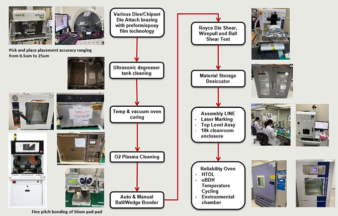
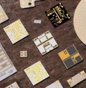
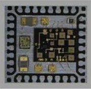
| Thin Film | LCC Package | Lead Frame |
Various transceiver, 65Ghz HPA packages DA/WB, sub-mount and full assembly |
|
Bonding Process and Equipment
On our 22,000 square feet facility, apart from being a RF, microwave and millimeter-wave design expert, we have extended our capabilities and services to provide a full bonding solution to support our customers on the challenging Semiconductor bonding market.
In-house, we have production line that is doing manufacturing, equipment assembly line, a R&D engineering room, bonding, and test lab We provide PCB design by generating layout, schematics up to PCB fabrication and PCB testing. We do mechanical design as well by designing jig, fixtures up till tools fabrication to support our customer process and machinery. We processed PCBA and sub-mount all the way starting from SMT to Frontend on the DA/WB to Backend assembly where we assemble all the parts and final product testing.